- Understanding Intel CPU Names and Numbers
- Early Intel Processor Generations
- The Dawn of Pentium and Beyond
- 1993: Pentium (P5, i586)
- 1994-99: Intel Pentium III Processor and the Problems That Preceded It
- 1995: Pentium Pro (P6, i686)
- 1997: Pentium II and Pentium II Xeon
- 1998: Celeron
- 1999: Pentium III and Pentium III Xeon
- 2000: Pentium 4
- 2001: Xeon
- 2001: Itanium
- 2002: Hyper-Threading
- 2003: Pentium M
- 2005: Pentium D
- 2006: Core 2 Duo
- 2007: Intel vPro
- The Modern Intel Processor Generations
- Conclusion
- FAQ
The evolution of Intel processors is a fascinating history.
In 1968, Gordon Moore went to Bob Noyce’s house to have a conversation where they talked about the state of their current jobs and the potential for a new company.
This fateful encounter led to the birth of Intel on July 18, 1968. The company would change the face of technology for years to come.
Let’s begin.
Understanding Intel CPU Names and Numbers
Let’s first discuss the specifics of what each Intel CPU model means before moving on to the timeline of Intel processors.
The model name has numerous numbers and letters, which can be confusing.
Each Intel processor has the following details:
Brand: This refers to the entire range of products, including Core, Pentium, Xeon, and Celeron.
Brand modifier: It describes the processor’s performance under that particular brand. A brand modifier’s value increases with its performance. For example, i3, i5, i7, and i9.
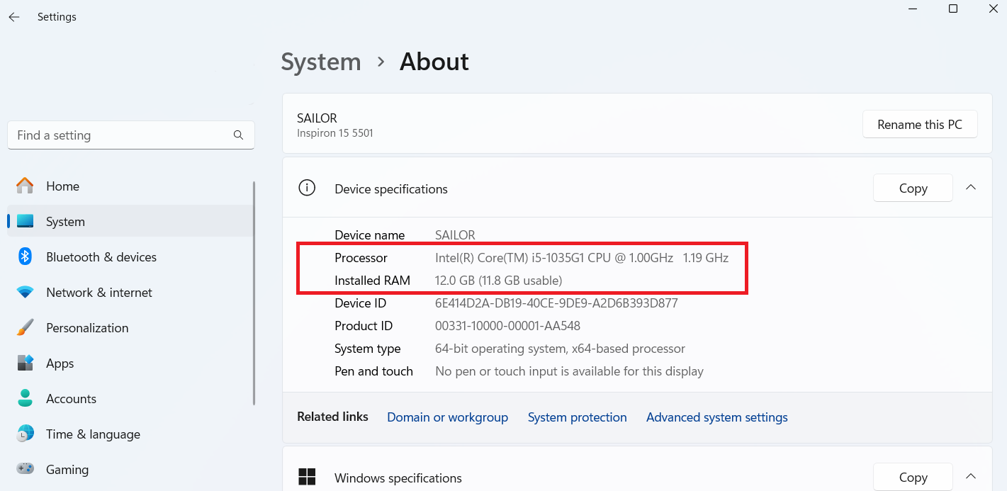
Generation indicator: The first one or two digits of the processor number represent the CPU’s generation. For example, from the screenshot above, you’ll see “Core i5-1035G1.” The “1” stands for the 1st generation.
SKU: This refers to the final three processor number digits. When the SKU is higher, it means the processor has more features included. The SKU from the Core i5-1035G1 is the “035.”
Suffix for product lines: The last letter of “Core i5-1035G1” is “G1.” It’s the features of the CPU. Some of the Intel Core’s product line suffixes include “H” for high-performance graphics, “K” for overclocking unlocked, “C” for desktop processors with high-end graphics, etc.
Early Intel Processor Generations
The evolution of processors developed by Intel has significantly improved across generations. The key change between each generation is the architecture.
With time, Intel improved its overclocking, cache, and RAM support. Newer CPUs achieved higher clock speeds and more energy efficiency.
Let’s now examine the Intel processors timeline and other relevant information.
![IMG]() 1971-81: The 4004, 8008, and 8800
1971-81: The 4004, 8008, and 8800

Intel processors underwent massive innovation in the 1970s, from which came the 4004, 8008, and 8800.
These processors significantly influenced how computing technology developed in the future.
Intel 4004
When Intel released the 4004, it transformed the market by combining all CPU operations onto a single chip. It was the first processor to be sold commercially.
The Intel 4004 had 2,300 transistors and could process clock speeds between 108 and 740 kHz. This resulted in a performance of 0.07 million instructions per second (MIPS).
Clock speed is measured in hertz (Hz), with gigahertz (GHz) and megahertz (MHz) being typical prefixes. One million cycles per second equals one megahertz, while one billion cycles per second equals one gigahertz. A faster clock speed CPU usually means the computer can quickly process information.
Intel 8008
The 8008 followed the 4004 with 3,500 transistors and a clock speed of 0.5 to 0.8 MHz and was primarily used in the Texas Instruments 742 computer. It was released in 1972.
Intel 8080
Intel released the 8080 in 1974 with 4,500 transistors and a clock speed of up to 2 MHz. The 8080 was used in the AGM-86 cruise missile manufactured by Boeing.
It was also well-known for its use in the Altair 8800 microcomputer kit.
| Processor | Clock Speed | Transistors | Performance (MIPS) |
| Intel 4004 | 108 kHz – 740 kHz | 2,300 | 0.07 |
| Intel 8008 | 0.5 MHz – 0.8 MHz | 3,500 | N/A |
| Intel 8800 | Up to 2 MHz | 4,500 | N/A |
![IMG]() 1978-82: iAPX 86 (8086), 8088, and 80186 (16-bit)
1978-82: iAPX 86 (8086), 8088, and 80186 (16-bit)
Other Intel processors listed by generation are the iAPX 86 (8086), 8088, and 80186 (16-bit).
The release of the iAPX 86 (8086) and its models between 1978 and 1982 was a significant turning point in Intel’s processor development.
When the iAPX 86 (8086) was introduced in 1978, Intel’s first 16-bit CPU was available for sale. It had 29,000 transistors and a clock speed of 5 to 10 MHz.
This chip helped establish the enduring x86 architecture, which boosted Intel’s market dominance.
In 1978, Intel simultaneously debuted the 8088, almost the same as the 8086 but with an 8-bit internal bus.
The 8088 played a crucial role in the first IBM PC, a turning point in the history of personal computing.
| Processor | Transistors | Applications | Clock Speed (MHz) |
| iAPX 86 (8086) | 29,000 | IBM PS/2, computers | 5-10 |
| 80186 | 2,000 | Embedded systems | Over 1 |
| 8088 | 29,000 | IBM PC | 5-10 |
![IMG]() 1981: iAPX 432
1981: iAPX 432
The iAPX 432 is one of the Intel processor generations that was less successful. The 432 debuted in 1981 and was Intel’s first attempt at 32-bit design.
It had an incredibly complex architecture with integrated memory management and multitasking.
Despite its complexity, this processor’s production costs made it unpopular and limited its commercial appeal because it was slower than the new 80286 architecture.
The 432 project was initially meant to replace the 8086 series. It ended in 1982, but it helped Intel refine and advance its CPU designs.
![IMG]() 1982: 80286
1982: 80286
When the Intel 80286 was released, it had improved memory management and strong security features.
By 1991, it was achieving clock speeds as high as 25 MHz, with performance that surpassed 4 MIPS.
This CPU had 134,000 transistors and a 1,500 nm manufacturing scale and was widely used in IBM-PC AT and AT PC clones.
It was one of Intel’s most economical chips in the evolution of Intel processors.
This change reflects the continuous advancement of manufacturing processes, which make it possible to produce increasingly complex and smaller components.
For instance, the size of transistors and other features on a chip is usually measured in nanometers when discussing integrated circuits and processors.
The change from micrometers to nanometers makes developing densely packed and efficient electronic components possible. This helps to create smaller and more powerful devices.
The 80286 is still remembered as a turning point in the history of Intel processors because of the massive performance increase over the previous generation.
In 2007, Intel said that the new Atom CPU was the only one in the Intel processors list by generation that could match the 80286’s cost-effectiveness after 25 years.
This made it the best option for people and companies looking to upgrade their computer systems without spending much money.
| Processor | Clock Speed | Transistor Count | Performance (MIPS) |
| 80286 | 6-25 MHz | 134,000 | 4+ |
| 80186 | 6-10 MHz | 55,000 | 1+ |
| 8088 | 5-10 MHz | 29,000 | 1+ |
| 8086 | 5-10 MHz | 29,000 | 1+ |
![IMG]() 1985-94: 386 and 376
1985-94: 386 and 376
The 386DX CPU was released in 1985 and had 275,000 transistors (1,500 nm) with clock rates ranging from 16 to 33 MHz to achieve up to 11.4 MIPS.
A higher MIPS score generally means better performance, but remember that MIPS alone doesn’t give a whole picture of a processor’s capabilities. Overall performance is also greatly influenced by other elements, including clock speed, architecture, and the type of instructions.
This was the beginning of the 32-bit era in the history of Intel processors . The 386SX was released in 1988.
The processor had a 1,000 nm design and a 16-bit bus for mobile and affordable desktop systems. Both used the 80287 until the 80387 was released, and neither had a math coprocessor.
Intel’s 386SL (1990) was the company’s first notebook processor with its on-chip cache, controller, and 855,000 transistors.
Intel Boosted Its Notebook Market Share
Intel increased its market share in the notebook sector. This processor was designed for mobile devices and was focused on low-power operation to extend battery life.
It had clock speeds between 20 and 25 MHz. The 376/386 family for embedded systems was completed with the 386EX (1994) and 376 (1989).
Due to demand in embedded and aerospace applications, Intel continued to build the 80386 series until September 2007, even though it was no longer necessary for consumer computers.
| Processor | MIPS | Clock Speed (MHz) | Transistors |
| 386SX | 8.7 | 16-33 | 275,000-1.2 million |
| 386DX | 11.4 | 16-33 | “ |
| 386SL | 5.6 | 20-25 | “ |
| 386EX | 7.8 | 16-33 | “ |
In the evolution of processors , the 386SL paved the way for portable computing.
![IMG]() 1989: 486 and i860
1989: 486 and i860
Intel’s introduction of the 486 CPU in 1989 was a major improvement in the history of Intel processors.
This microprocessor became Intel’s most popular and successful chip and transformed personal computing with 70.7 MIPS and clock speeds between 25 to 100 MHz.
Intel released the i860 processor at the same time to break into the Reduced Instruction Set Computing (RISC) processor industry.
However, the i860 and its replacement, the i960, weren’t successful, even with the benefits of quickly processing basic commands.
This caused Intel to shift its attention to the widely used x86 architecture.
In a 32-bit architecture, the processor can handle data in 32-bit chunks. This means it can process up to 32 bits of data at once. It was usually designed for older hardware and software.
In a 64-bit architecture, the CPU can handle data in 64-bit chunks. This means that more data can be processed at once and that memory addresses can be substantially larger.
The Dawn of Pentium and Beyond
Intel introduced Pentium in 1993, and it became a vital part of the history of Intel processors.
Intel reportedly changed to Pentium because of the protection of the trademark against AMD, which named its processors 486.
However, Pentium processors transformed the computing industry with their powerful performance and advanced multimedia features.
It set a new standard for personal computing and prepared the way for further Intel processor generations.
Here’s the Intel processors timeline for Pentium:
![IMG]() 1993: Pentium (P5, i586)
1993: Pentium (P5, i586)
The P5 Pentium was released in 1993 at 60 MHz, reaching 200 MHz (P54CS) in 1996. 3.1 million transistors were included in the first 800 nm design.
This number increased to 3.3 million in the 1996 version with a smaller 350 nm scale.
When the P55C (multimedia extensions) was released in 1997, the processor’s architecture was improved to include 4.5 million transistors and a 233 MHz clock speed.
The Pentium MMX mobile model was available, with a top speed of 300 MHz until 1999.
Over the Intel processors timeline, they kept improving the Pentium brand by adding new features and raising clock speeds in each generation.
The company reached a turning point in 1997 with the release of the Pentium MMX. This added specialized instructions for multimedia processing and improved multimedia performance.
This advancement particularly improved image editing, ensured smooth video playback, and increased the immersive quality of games.
![IMG]() 1994-99: Intel Pentium III Processor and the Problems That Preceded It
1994-99: Intel Pentium III Processor and the Problems That Preceded It
Intel suffered a major setback in 1994 when a professor at Lynchburg College found a problem with the Pentium processor.
The Pentium FDIV bug caused division results for particular operations to be inaccurate, which led to considerable criticism and damaged Intel’s reputation.
It was one of the major setbacks in the history of Intel processors. However, the company quickly resolved the problem and offered free replacements to impacted users.
After five years, Intel released the Pentium III CPU in 1999. This launch had a CPU Serial Number (PSN) for unique identification.
This identification caused privacy concerns among consumers of possible unlawful tracking. As a result of these concerns, Intel stopped embedding the PSN feature in its processors.
![IMG]() 1995: Pentium Pro (P6, i686)
1995: Pentium Pro (P6, i686)
Most people misunderstood the Pentium Pro, but it wasn’t meant to replace the Pentium 5.
It was supposed to serve as a workstation and server workload-focused predecessor to the Pentium II Xeon.
The Pentium Pro, built-in 350 nm, included 5.5 million transistors and multiple models with speeds ranging from 150 to 200 MHz.
Its unique design allowed for out-of-order execution, and its 36-bit address bus supported up to 64 GB of memory.
It achieved popularity by breaking the 1 teraflop performance barrier on the ASCI Red supercomputer.
![IMG]() 1997: Pentium II and Pentium II Xeon
1997: Pentium II and Pentium II Xeon
Based on the 6th-generation P6 architecture, the Pentium II CPU was designed primarily for consumers.
It broke from the conventional socket devices and introduced a slot module resembling a cartridge.
It addressed problems from the first P6 version and significantly improved 16-bit execution with 7.5 million transistors (2 million more than the P6).
The Pentium II kept the MMX instruction set from the Pentium, the Pentium II’s predecessor. The Pentium II was first released with the 350 nm Klamath core (233 and 266 MHz).
However, in 1998, it was upgraded to a 250 nm Deschutes core, which could reach clock speeds of 450 MHz. It also offered a Pentium II Overdrive for Pentium Pro upgrades.
Both the 250 nm/180 nm Dixon and 250 nm Tonga cores were used in mobile Pentium II processors.
![IMG]() 1998: Celeron
1998: Celeron
Even though Celerons use modern processing technology, they usually have significant downgrades, such as less cache memory, and are only suitable for simple PC applications.
Intel can compete in the entry-level PC market thanks to Celerons. The frequency range is 266 to 300 MHz for desktops and up to 500 MHz for mobile.
So, the original Celeron series used the 250 nm Covington core for desktop computers and the 250 nm Mendocino core (19 million transistors, including L2 on-die cache) for laptop computers.
Modern Celerons are continually updated, and their architecture is derived from Sandy Bridge.
![IMG]() 1999: Pentium III and Pentium III Xeon
1999: Pentium III and Pentium III Xeon
In the evolution of Intel processors, the company joined AMD in the gigahertz race and answered Transmeta’s low-power challenge with the release of the Pentium III in 1999.
First, it had a 250 nm Katmai core. After that, it had 180 nm Coppermine and Coppermine T cores and 130 nm Tualatin cores.
Because of the integrated L2 cache, the transistor count grew from 9.5 million in Katmai to 28.1 million. With Tualatin, clock frequencies varied from 450 MHz to 1,400 MHz.
The first gigahertz versions of Intel were rushed out, which prompted a recall and rerelease. Intel was criticized for this.
SpeedStep, which enables CPU clock speed scaling, was first presented to consumers with the Mobile Pentium III in 2000.
Its introduction, which came soon after the Transmeta Crusoe CPU was unveiled, raised rumors of competitive pressure.
Associated with the Pentium name, the Pentium III Xeon debuted in 1999 alongside the Tanner core.
Although higher gigahertz values were believed to correspond to improved performance, this method had drawbacks, including more power and heat generation.
Eventually, both companies shifted their focus to introducing more cores, increasing efficiency, and improving processor architecture overall. Today’s CPU performance evaluation takes a more comprehensive approach, considering factors more than just clock speed.
![IMG]() 2000: Pentium 4
2000: Pentium 4
In 2000, the Pentium 4 marked a pivotal shift in the timeline of Intel processors. It was launched with the 180 nm Willamette core (42 million transistors).
The Netburst architecture planned for clock speed scalability, envisioning 20 GHz by 2010. However, limitations occurred as current leakage and power consumption increased rapidly with higher clock speeds.
Starting at 1.3 GHz, it reached 3.8 GHz with the 90 nm Prescott core (125 million transistors) in 2005.
The Pentium 4 series grew complex with models like Mobile Pentium 4-M, Pentium 4E HT (Hyper-Threading), and Pentium 4F (65 nm Cedar Mill core) in 2005.
Tejas, intended to replace Pentium 4, was canceled, leading to the Core architecture. This led to a significant efficiency-focused shift in the evolution of processors.
![IMG]() 2001: Xeon
2001: Xeon
With a 180 nm Foster core and clock speeds ranging from 1.4 to 2 GHz, the Netburst architecture was used in the first Xeon without the Pentium brand.
The Netburst architecture continued until 2006, when a complete portfolio of Xeon processors with different core counts, including Nocona, Irwindale, Cranford, Potomac, Paxville, Dempsey, and Tulsa, was introduced.
Intel redesigned its architecture in response to concerns about power consumption, completing the Netburst Xeons with the dual-core Dempsey CPU.
Based on the 32 nm Sandy Bridge and Sandy Bridge-EP architecture, modern Xeons have up to 10 cores, 3.46 GHz clock rates, and up to 2.6 billion transistors.
![IMG]() 2001: Itanium
2001: Itanium
The Itanium was modeled after the i860 and iAPX 432 principles and was misunderstood for a long time.
Despite early doubts, it was backed by powerful supporters and its use was continued.
When the Itanium was introduced in 2001 as Intel’s first 64-bit CPU, its 32-bit performance constraints drew criticism.
With 320 million transistors and clock frequencies of 733 MHz and 800 MHz, the 180 nm Merced core debuted.
First released in 2002, the Itanium 2 saw only irregular updates until 2010.
Its cores included McKinley, Madison, Deerfield, Hondo, Fanwood, Montecito, Montvale, and Tukwila, with over 2 billion transistors and a large 24 MB on-die cache.
![IMG]() 2002: Hyper-Threading
2002: Hyper-Threading
In 2002, Intel made a breakthrough in the evolution of processors in desktop CPUs by introducing Hyper-Threading Technology.
Hyper-Threading was first introduced in Xeon and Pentium 4 CPUs, which allows two threads to run simultaneously and can improve speed by as much as 30%.
This technology continues to be present in later Intel processors, such as the Pentium D, Atom, Core i-Series, and Itanium CPUs, and it helps to enhance processing power.
This improves efficiency and resource usage overall and enables the CPU to tackle numerous tasks simultaneously. AMD refers to its implementation as Simultaneous Multithreading (SMT), while Intel calls it Hyper-Threading Technology (HTT).
📌 Related: How to Check What CPU Do I Have on My Windows PC?
![IMG]() 2003: Pentium M
2003: Pentium M
With the 130 nm Banias core, which consumes less power, Intel released the Pentium M 700 series in 2003 for mobile computing.
This processor stressed power efficiency over clock speed, thanks to the leadership of Mooly Eden’s Israeli design team.
Banias’ TDP was lowered to 24.5 watts with clock speeds ranging from 900 MHz to 1.7 GHz, a considerable reduction over the 88 watts of the Pentium 4 Mobile.
The 90 nm Dothan version, which has 140 million transistors and clock rates of up to 2.13 GHz, further reduced TDP to 21 watts.
After Dothan was replaced, Yonah developed into the Core Duo and Core Solo in 2006, influencing Intel’s future in a manner akin to that of the 4004, 8086, and 386.
![IMG]() 2005: Pentium D
2005: Pentium D
The Pentium D was one of the Intel processor generation’s first dual-core CPUs released in 2005.
The first edition of the Pentium D 800 series used the Smithfield core, a 90 nm version of two Northwood cores while keeping the Netburst architecture.
Later, it became the 65 nm Presler with two Cedar Mill cores.
Extreme Editions were produced with a record-breaking 130 watts of power consumption for consumer desktop CPUs (with server processors reaching 170 watts).
It capped the maximum clock speed at 3.73 MHz. Prescott has 376 million transistors, compared to Smithfield’s 230 million.
![IMG]() 2006: Core 2 Duo
2006: Core 2 Duo
Intel’s reaction to AMD’s popular Athlon X2 and Opteron processors was the Core 2 Duo.
Intel quickly released quad-core models after releasing the 65 nm Conroe desktop processor, the T7000 series, and the Xeon 5100 series.
The company underwent a major restructuring and repositioning due to this microarchitecture change.
In 2006, Conroe reclaimed its performance leadership with clock speeds ranging from 1.2 GHz to 3 GHz and 291 million transistors.
Later, in 2008, the CPUs experienced a 45 nm Penryn downsizing to match Intel’s tick-tock cadence.
![IMG]() 2007: Intel vPro
2007: Intel vPro
In 2007, Intel released vPro, a promotional term with hardware innovations integrated into specific processors.
With technologies like Hyper-Threading, Active Management Technology (AMT), Turbo Boost 2.0, and VT-x all bundled into one package, vPro was primarily meant for enterprise use.
A system has to have a CPU, chipset, and BIOS that support vPro technology to use vPro. Among the technologies found in vPro is Virtualization Technology (VT).
It’s a hardware-based solution for running multiple workloads in isolation with less performance overhead than software virtualization.
Another one is the Trusted Execution Technology (TXT), which builds a secure trust chain and ensures computer authenticity using the Trusted Platform Module (TPM).
The last one is the Active Management Technology (AMT), which makes remote access and management possible even when the computer is off.
The Modern Intel Processor Generations
Below is the timeline of Intel processors from the current generations:
![IMG]() 2008: Core i-Series
2008: Core i-Series
Intel released the Core i3, i5, and i7 processors in 2008 using the Nehalem microarchitecture and a 45 nm manufacturing process.
The Celeron, Pentium Core, and Xeon brands of Intel CPUs were built on this architecture, which was later scaled down to 32 nm in 2010.
The Westmere architecture could support up to eight cores with clock speeds up to 3.33 GHz and 2.3 billion transistors.
![IMG]() 2010: Core i3, i5, i7 Processors
2010: Core i3, i5, i7 Processors
Intel released the new Intel Core series of CPUs, which included Intel Turbo Boost Technology for laptops, desktops, and integrated devices in 2010.
The new Intel processor generations now included integration and smart performance.
With the introduction came new Intel Core i7, i5, and i3 CPUs, the company’s 32-nanometer (nm) manufacturing process making its release.
For the first time, high-definition graphics were integrated into a processor, built and delivered by Intel.
The 32nm technology and second-generation high-k metal gate transistors were featured in the 2010 Intel Core processors and included more than 25 platform products.
This improved speed and decreased energy usage.
![IMG]() 2012: Intel SoCs
2012: Intel SoCs
Intel introduced their Atom SoCs to the system-on-a-chip (SoC) industry in the middle of 2012. Although based on older CPUs, the first Atom SoCs had trouble competing with ARM-based rivals.
The release of the 22nm Silvermont-based Baytrail Atom SoCs in late 2013 marked a turning point.
With TDPs as low as 4 watts, these genuine SoCs, like Avoton for servers, included every component needed for tablets and laptops.
Intel entered the high-end tablet market in 2014 when it released ultra low-power Haswell architecture Y SKU suffix CPUs.
![IMG]() 2013: Core i-Series – Haswell
2013: Core i-Series – Haswell
The Sandy Bridge architecture was replaced by the 22nm Haswell microarchitecture when Intel refreshed its Core i-Series in 2013.
For low-power CPUs (10- to 15-watt TDP) seen in ultrabooks and high-end tablets, Haswell introduced the Y SKU suffix.
The Haswell-EP Xeon CPUs had 5.69 billion transistors and up to 18 cores, with clock frequencies of up to 4.4 GHz.
The Devil’s Canyon refresh, which improved clock rates and thermal interface material, was released by Intel in 2014.
Except for entry-level desktop CPUs, the 2014 Broadwell die shrink to 14nm coexisted with Haswell CPUs.
![IMG]() 2015: Broadwell
2015: Broadwell
In 2015, the fourth generation of processors had a default architecture that moved to 14nm.
With a 37% smaller footprint than its predecessor, Broadwell offered faster wake times and a 1.5-hour longer battery life.
Also, it improved graphics performance by using 1150 LGA sockets to support two-channel DDR3L-1333/1600 RAM.
![IMG]() 2016: Kaby Lake
2016: Kaby Lake
Kaby Lake was the first Intel processor that deviated from the “tick-tock” model. It introduced faster CPU clock speeds and modifications while keeping IPC values the same.
It was significant since it was the first time Intel hardware was incompatible with Windows 8 or earlier.
Except for Xeon, it powered Core, Pentium, and Celeron CPUs and excelled at processing 4K videos. In early 2017, Intel released the R versions that supported DDR4-2666 RAM.
![IMG]() 2017: Ice Lake
2017: Ice Lake
Following the release of the Core-based Coffee Lake, Intel released the 10th generation Ice Lake in 2017.
With its 10 nm technology, the Ice Lake design introduced Thunderbolt 3 and Wi-Fi 6 support, highlighting increased connectivity and transfer speeds.
With a maximum CPU clock rate of 3.7GHz and up to 40 cores, the SP model, which comes in Core and Xeon processor varieties, launched in April 2021 and achieved a processing speed of over 1 teraflops.
Since 2021, Xeon Silver, Gold, and Platinum models have been available. However, the 2019 Intel Core i3/i5/i7 processors are still available.
![IMG]() 2020: Tiger Lake
2020: Tiger Lake
The Tiger Lake series of mobile processors from Intel replaces the Ice Lake series. These CPUs are the first to jointly promote the Celeron, Pentium, Core, and Xeon brands since Skylake.
They come in dual- and quad-core models. The Tiger Lake chips are designed specifically for thin gaming laptops and offer a maximum refresh rate of 100 frames per second.
The Core i9-11980HK has a maximum boost clock speed of 5 GHz.
![IMG]() 2021: Alder Lake
2021: Alder Lake
Alder Lake is a major advancement with its cutting-edge hybrid architecture that combines powerful P-cores (Golden Cove Performance cores) and effective E-cores (Gracemont high-efficiency cores) in a single package.
This architecture preserves energy efficiency while enabling higher performance than traditional CPUs.
Alder Lake introduces the new LGA 1700 Socket, which includes Wi-Fi 6E and Thunderbolt 4.
Enhancing game performance and energy efficiency is Alder Lake’s top priority, with an 18% IPC boost over the previous generation.
📌 Related: CPU Cores Explained: Do Cores Affect Performance?
![IMG]() 2022: Raptor Lake
2022: Raptor Lake
Raptor Lake uses a second-generation hybrid architecture with the new Raptor Coves for performance and Gracemont efficiency cores.
Raptor Lake processors use the LGA 1700 socket, just as Alder Lake ones, and they are 10 nm in size.
Raptor Lake CPUs represent a significant milestone for being the first Intel Core processors to enable up to 24 cores.
The LGA 1700 socket handles DDR5 RAM, which can run at up to 5600MHz.
![IMG]() 2023: Meteor Lake
2023: Meteor Lake
Intel’s Meteor Lake processors use the Redwood Cove cores for performance (P-cores) and the Crestmont cores for efficiency (E-cores).
These processors have chiplet designs with streamlined manufacturing, customization, faster production, and possible cost savings in mind.
The H-series and U-series processors in the Meteor Lake family have different core counts and clock rates optimized for performance and battery efficiency.
Meteor Lake integrates AI with Xe cores from the Arc GPU and a dedicated NPU. The AI performance is promising. It beats rival laptops with Intel processors in some benchmarks.
📌 Further reading: Intel 14th Gen Released: What’s New in the Latest Intel Processor?
Conclusion
We’ve covered the history of Intel processors in this guide. The development of Intel microprocessors has been amazing, with each new generation building on the successes of the previous one.
These microprocessors, which range from the revolutionary 4004 to the state-of-the-art Intel Core processors, have steadily increased power, efficiency, and versatility.
Microprocessor development is expected to continue exceptionally as cutting-edge technologies like artificial intelligence and machine learning gain traction.
These developments will significantly impact how computing is shaped in the future.